183d Polymer Nano-Texturing and Stochastic Nano-Patterning Using Plasma Processing
Plasma processing induces roughening of polymers at the nanoscale, and forces one to abandon the idea of a flat surface, after processing, commonly used at the macro and micro scales. Plasma induced roughening of polymers may have detrimental effects when fabricating an electronic nano-device, or may have beneficial effects when it imparts anti-reflective or superhydrophobic properties on surfaces to mention only three examples. Thus, roughness should be reduced in some cases, while it should be maximized or controlled in others. Plasma induced polymer nano-roughness control may thus lead to new nano-manufacturing processes and products. This paper summarizes the recent finding of our group on plasma processing of both organic and inorganic (Silicon-containing) polymers.Ā | |||||||||||
| |||||||||||
A Helicon Plasma reactor is used for polymer plasma processing. Fractal theory based nanometrology protocol has been developed for the analysis of AFM images of the etched surfaces. (1+1) and (2+1) Monte Carlo Simulations are used for the explanation of observed behaviour. | |||||||||||
| |||||||||||
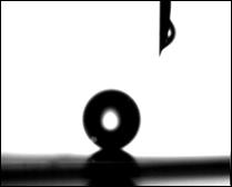
First, plasma nanotexturing has been used to control the wetting and reflectivity of polymer surfaces. Wettability and its control is an important feature of surface science and technology finding also new micro- and nano- scale applications such as droplet frictionless motion in microfluidics, biocompatibility tuning, protein and cell adsorption and others. Both very hydrophilic (VH) and super hydrophobic (SH) (self-cleaning) surfaces may be desirable. In addition to wetting control, other parameters such as optical properties should be also exactly controlled.Ā For polymers the production of SH, optically transparent, and antireflective surfaces is a very attractive objective. Wettability depends on both surface chemistry and topography. | |||||||||||
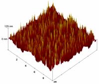
We developed a generic, fast, all-dry process for VH and SH surface production for organic and silicon- containing polymers. The organic polymer such as PMMA, PEEK, PS, PET sheet is loaded in a low-pressure reactor equipped with a Figure 1 PMMA nanotexturing in O2 plasmas, and Supehydrophobic (SH) Surface production . From Left to Right: Nanoroughness (RMS) versus etch time.Ā Contact angle and contact angle hysteresis after plasma deposition of fluorocarbon (FC) thin layer. Morphology of the surface after 1min etching time. Conditions: 2000 W source power, 0.75 Pa, 100 sccm, -100 V bias, 10 oC | |||||||||||
| |||||||||||
ĀWhen an organosilicon polymer such as PDMS is etched in SF6 plasma (instead of Oxygen) high aspect ratio nanostructures are also created. After plasma deposition of a thin fluorocarbon layer, these surfaces become SH as well.
| |||||||||||
| |||||||||||
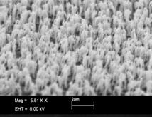
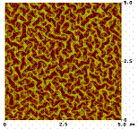
Inorganic polymers treated with SF6 plasmas gave high Aspect Ratio Nanopillar like morphology. However, for the same polymers ripple-like and periodic morphology was produced on O2 plasma etched PDMS (see top left figure 3), leading to sticky ¢ hydrophobic surfaces most of the times after fluorocarbon deposition. We have also demonstrated 2-10 fold increase of protein adsorption on such nanotextured surfaces. | |||||||||||
| |||||||||||
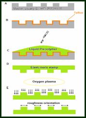
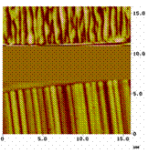
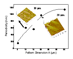
In all the above applications nanotexture but not nanopattern has been achieved. Could we do nanopatterning with plasmas? The answer to the question is yes, and we show an example below. A plasma-based methodology to fabricate oriented spontaneously formed nanostructures on Poly(dimethylsiloxane) PDMS films and stamps was discovered. Oxygen plasma treatment of PDMS produces spontaneously-formed wavy structures with high nano-scale amplitude and with periodicity of a few 100's nm as revealed by Atomic Force Microscopy (AFM). These nanostructures may be produced by two methods. a) In the first method, a stencil mask was placed on top of a thin PDMS film and O2 plasma treatment followed. b) In the second method, an elastomeric stamp was prepared by casting Sylgard 184 elastomer (Dow Corning) over lithographically created masters and then treated in O2 plasma. The dimensions of the elastomeric stamp determine the wavelength of the periodic nanostructures formed (see fig. 3)
| |||||||||||
| |||||||||||
This simple oxygen plasma treatment to orient spontaneously formed nanostructures, with wavelength in the sub-micrometer range, may be used to print, for example, fine patterns of biologically active molecules onto surfaces with high spatial frequency.
| |||||||||||
| |||||||||||
We will also demonstrate plasma-based nanodot formation on polymers, and propose plasma driven self-assembly processes. | |||||||||||
| |||||||||||
| |||||||||||
| |||||||||||
In conclusion, plasma processing proves to be an attractive path to nanotexture surfaces of polymers for various applications, and for nanopattern formation in a stochastic periodic manner. | |||||||||||
| |||||||||||
References
| |||||||||||
[1] Katerina Tsougeni, George Boulousis, Evangelos Gogolides and Angeliki Tserepi Oriented spontaneously formed nanostructures on Poly(dimethylsiloxane) films and stamps treated in O2 plasmas In Press, available on Line,Ā Microelectronic Egineering 2008,
| |||||||||||
[2] Tsougeni K, Tserepi A, Boulousis G, V. Constantoudis, E. Gogolides. ōTunable poly(dimethylsiloxane) topography in O2 or Ar plasmas for controlling surface wetting properties and their ageingö, (2007) JPN J Applied Physics 1 46 (2): 744-750. | |||||||||||
[3] Tsougeni K., Tserepi A., Boulousis G., Constantoudis V., Gogolides E. ōControl of nanotexture and wetting properties of polydimethylsiloxane from very hydrophobic to super-hydrophobic by plasma processingö, (2007) Plasma Processes and Polymers, 4 (4), pp. 398-405. | |||||||||||
[4] Vlachopoulou M.-E., Tserepi A., Beltsios K., Boulousis G., Gogolides E. ōNanostructuring of PDMS surfaces: Dependence on casting solventsö, (2007) Microelectronic Engineering, 84 (5-8), pp. 1476-1479. | |||||||||||
[5] Vourdas N., Tserepi A., Gogolides E. ōNanotextured super-hydrophobic transparent poly(methyl methacrylate) surfaces using high-density plasma processingö, (2007) Nanotechnology, 18 (12), art. no. 125304. | |||||||||||
[6] Tserepi A.D., Vlachopoulou M.-E., Gogolides E. ōNanotexturing of poly(dimethylsiloxane) in plasmas for creating robust superhydrophobic surfacesö(2006) Nanotechnology, 17 (15), art. no. 062, pp. 3977-3983. | |||||||||||
[7] Gogolides E., Constantoudis V., Patsis G.P., Tserepi A. ōA review of line edge roughness and surface nanotexture resulting from patterning processesö, (2006) Microelectronic Engineering, 83 (4-9 SPEC. ISS.), pp. 1067-1072. | |||||||||||
[8] Tserepi A., Gogolides E., Misiakos K., Vlachopoulou M.-E., Vourdas N., Greek Patent application number 20050100473; PCT application number GR 2006 / 000011. | |||||||||||
| |||||||||||

Web Page: www.imel.demokritos.gr/plasmagroup